NAVIGATION / MULTI INFO DISPLAY NAVIGATION SYSTEM Parking Brake Switch Circuit
DESCRIPTION
This circuit includes the parking brake switch assembly and radio and display receiver assembly.
WIRING DIAGRAM
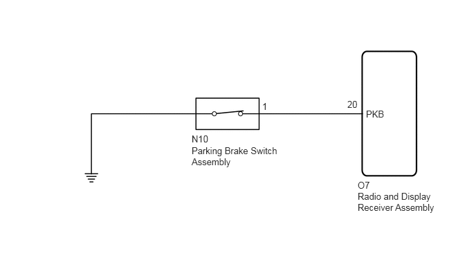
PROCEDURE
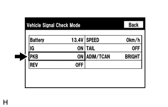
Display the "Vehicle Signal Check Mode" screen.
Check that the display changes between ON and OFF according to the parking brake operation.
- OK:
Parking Brake Condition Display Applied ON Released OFF
- HINT:
-
This display is updated once per second. As a result, it is normal for the display to lag behind the actual parking brake operation.
- Result:
Proceed to OK NG
OK
NG
Disconnect the O7 radio and display receiver assembly connector.
Disconnect the N10 parking brake switch assembly connector.
Measure the resistance according to the value(s) in the table below.
- Standard Resistance:
Tester Connection Condition Specified Condition O7-20 (PKB) - N10-1 Always Below 1 Ω
- Result:
Proceed to OK NG
OK
NG
Remove the parking brake switch assembly.
Click hereBrake>PARKING BRAKE>PARKING BRAKE SWITCH>REMOVAL201902,999999,_54,_078671,_0381559,RM100000001G0O2,
Inspect the parking brake switch assembly.
- Result:
Proceed to OK NG
OK
NG
Click hereBrake>PARKING BRAKE>PARKING BRAKE SWITCH>REMOVAL201902,999999,_54,_078671,_0381559,RM100000001G0O2,