☰ Toyota HiAce☰ فهرستAudio / Visual / Telematics › AUDIO / VIDEO › AUDIO AND VISUAL SYSTEM(for Radio and Display Type)
RM35X0E
_56
Audio / Visual / Telematics
_078377
AUDIO / VIDEO
_0385463
AUDIO AND VISUAL SYSTEM(for Radio and Display Type)
J
AUDIO / VIDEO AUDIO AND VISUAL SYSTEM(for Radio and Display Type) Data Signal Circuit between Radio Receiver and Stereo Jack Adapter
DESCRIPTION
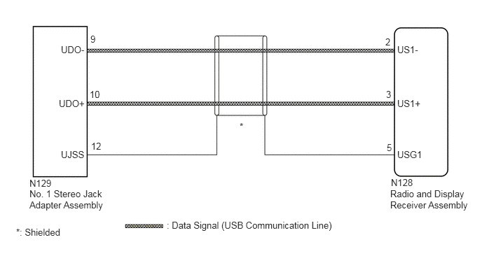
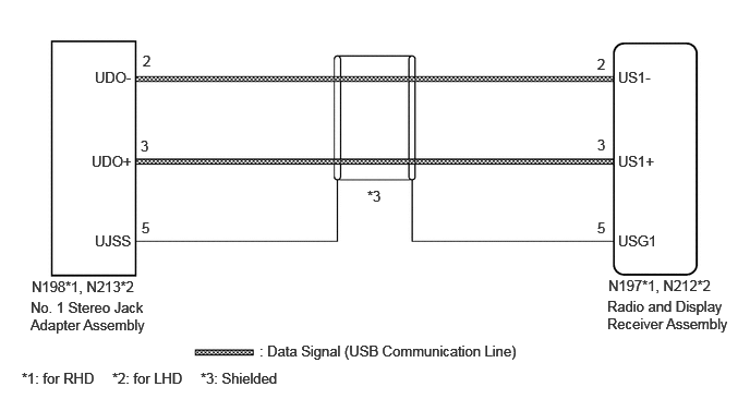
The No. 1 stereo jack adapter assembly sends the sound data signal or image data signal from a USB device to the radio and display receiver assembly via this circuit.
WIRING DIAGRAM
w/ AUX Function
1.344,0.5 1.521,0.677
0.177,0.177
10
false
9
0.875,1.458 1.49,1.656
0.615,0.198
10
false
UDO+
0.906,2.219 1.521,2.417
0.615,0.198
10
false
UJSS
5.906,2.219 6.521,2.417
0.615,0.198
10
false
USG1
5.906,1.458 6.521,1.656
0.615,0.198
10
false
US1+
5.906,0.656 6.521,0.854
0.615,0.198
10
false
US1-
0.438,2.646 1.052,2.844
0.615,0.198
10
false
N129
0.438,2.802 1.594,3.281
1.156,0.479
10
false
No. 1 Stereo Jack Adapter Assembly
2.479,3.271 5.083,3.5
2.604,0.229
10
false
: Data Signal (USB Communication Line)
0.24,3.375 1.458,3.646
1.219,0.271
10
false
*: Shielded
5.813,2.635 6.427,2.833
0.615,0.198
10
false
N128
5.802,2.802 7,3.271
1.198,0.469
10
false
Radio and Display Receiver Assembly
5.729,0.542 5.906,0.719
0.177,0.177
10
false
2
1.333,1.323 1.51,1.5
0.177,0.177
10
false
10
1.354,2.094 1.531,2.271
0.177,0.177
10
false
12
5.75,2.115 5.927,2.292
0.177,0.177
10
false
5
5.74,1.323 5.917,1.5
0.177,0.177
10
false
3
0.906,0.656 1.521,0.854
0.615,0.198
10
false
UDO-
3.563,1.802 4.781,2.073
1.219,0.271
10
false
*
w/o AUX Function
1.365,0.5 2.094,0.708
0.729,0.208
10
false
2
0.875,1.458 1.49,1.656
0.615,0.198
10
false
UDO+
0.906,2.219 1.521,2.417
0.615,0.198
10
false
UJSS
5.906,2.219 6.521,2.417
0.615,0.198
10
false
USG1
5.906,1.458 6.521,1.656
0.615,0.198
10
false
US1+
5.906,0.656 6.521,0.854
0.615,0.198
10
false
US1-
0.302,2.656 1.583,3.052
1.281,0.396
10
false
N198*1, N213*2
0.292,2.854 1.448,3.333
1.156,0.479
10
false
No. 1 Stereo Jack Adapter Assembly
2.479,3.271 5.083,3.5
2.604,0.229
10
false
: Data Signal (USB Communication Line)
1.917,3.531 3.135,3.802
1.219,0.271
10
false
*3: Shielded
5.813,2.646 7.083,2.813
1.271,0.167
10
false
N197*1, N212*2
5.802,2.844 7,3.313
1.198,0.469
10
false
Radio and Display Receiver Assembly
5.708,0.531 5.885,0.708
0.177,0.177
10
false
2
1.344,1.313 2.219,1.5
0.875,0.188
10
false
3
1.354,2.094 2.208,2.281
0.854,0.188
10
false
5
5.708,2.094 5.885,2.271
0.177,0.177
10
false
5
5.708,1.302 5.885,1.479
0.177,0.177
10
false
3
0.906,0.656 1.521,0.854
0.615,0.198
10
false
UDO-
3.51,1.792 4.729,2.063
1.219,0.271
10
false
*3
0.208,3.531 1.427,3.802
1.219,0.271
10
false
*1: for RHD
1.073,3.531 2.292,3.802
1.219,0.271
10
false
*2: for LHD
PROCEDURE
1.CHECK MODEL
a.
Choose the model to be inspected.
- Result:
Result Proceed to w/ AUX Function A w/o AUX Function B
A
2.CHECK HARNESS AND CONNECTOR (RADIO AND DISPLAY RECEIVER ASSEMBLY - NO. 1 STEREO JACK ADAPTER ASSEMBLY)
B
3.CHECK HARNESS AND CONNECTOR (RADIO AND DISPLAY RECEIVER ASSEMBLY - NO. 1 STEREO JACK ADAPTER ASSEMBLY)
2.CHECK HARNESS AND CONNECTOR (RADIO AND DISPLAY RECEIVER ASSEMBLY - NO. 1 STEREO JACK ADAPTER ASSEMBLY)
a.
1.542,2.198 1.979,2.49
0.438,0.292
1.542,0.208 1.958,0.479
0.417,0.271
2.135,1.938 1.781,1.49
true
1.844,1.354 2.26,1.5
true
1.115,1.667 1.583,1.313
true
1.417,4.083 1.656,3.76
true
0.969,4.063 1.646,3.667
true
2.135,4 1.792,3.656
true
0.24,0.188 0.552,0.385
0.313,0.198
10
false
*a
0.24,2.802 0.552,3
0.313,0.198
10
false
*b
0.76,1.625 1.188,1.833
0.427,0.208
10
false
US1+
2.188,1.906 2.677,2.146
0.49,0.24
10
false
USG1
2.313,1.438 2.729,1.688
0.417,0.25
10
false
US1-
0.635,4.021 1.031,4.281
0.396,0.26
10
false
UDO-
1.24,4.094 1.74,4.354
0.5,0.26
10
false
UJSS
2.167,3.938 2.604,4.198
0.438,0.26
10
false
UDO+
1.594,0.26 2.052,0.458
0.458,0.198
10
false
N128
1.615,2.26 2.188,2.573
0.573,0.313
10
false
N129
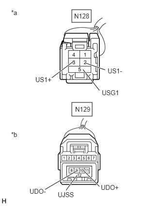
| *a | Front view of wire harness connector
(to Radio and Display Receiver Assembly) |
| *b | Front view of wire harness connector
(to No. 1 Stereo Jack Adapter Assembly) |
Disconnect the N128 radio and display receiver assembly connector.
b.
Disconnect the N129 No. 1 stereo jack adapter assembly connector.
c.
Measure the resistance according to the value(s) in the table below.
- Standard Resistance:
Tester Connection Condition Specified Condition N128-2 (US1-) - N129-9 (UDO-) Always Below 1 Ω N128-3 (US1+) - N129-10 (UDO+) Always Below 1 Ω N128-5 (USG1) - N129-12 (UJSS) Always Below 1 Ω N128-2 (US1-) or N129-9 (UDO-) - Body ground Always 10 kΩ or higher N128-3 (US1+) or N129-10 (UDO+) - Body ground Always 10 kΩ or higher N128-5 (USG1) or N129-12 (UJSS) - Body ground Always 10 kΩ or higher
- Result:
Proceed to OK NG
OK
PROCEED TO NEXT SUSPECTED AREA SHOWN IN PROBLEM SYMPTOMS TABLE
NG
REPAIR OR REPLACE HARNESS OR CONNECTOR
3.CHECK HARNESS AND CONNECTOR (RADIO AND DISPLAY RECEIVER ASSEMBLY - NO. 1 STEREO JACK ADAPTER ASSEMBLY)
*1: for RHD
*2: for LHD
a.

1,0.167 1.417,0.417
0.417,0.25
1.917,0.167 2.333,0.417
0.417,0.25
1,2 1.417,2.25
0.417,0.25
1.917,2 2.333,2.25
0.417,0.25
1.25,1.333 1.625,1.021
true
2.229,0.948 1.771,0.99
true
2.188,1.313 1.75,1.146
true
1.177,3.031 1.625,2.802
true
1.781,2.792 2.208,2.885
true
1.75,2.938 2.115,3.125
true
0.292,0.219 0.5,0.417
0.208,0.198
10
false
*a
0.323,2.094 0.531,2.292
0.208,0.198
10
false
*b
1.052,0.219 1.479,0.385
0.427,0.167
10
false
N197
0.896,1.333 1.281,1.51
0.385,0.177
10
false
US1+
2.302,0.875 2.719,1.042
0.417,0.167
10
false
US1-
2.25,1.26 2.667,1.427
0.417,0.167
10
false
USG1
0.75,2.979 1.177,3.146
0.427,0.167
10
false
UDO+
2.25,2.813 2.646,2.969
0.396,0.156
10
false
UDO-
2.146,3.094 2.563,3.26
0.417,0.167
10
false
USSS
1.958,0.208 2.385,0.375
0.427,0.167
10
false
N212
1.052,2.042 1.479,2.208
0.427,0.167
10
false
N198
1.958,2.031 2.385,2.198
0.427,0.167
10
false
N213
1.469,0.188 1.677,0.385
0.208,0.198
10
false
*A
2.375,0.188 2.583,0.385
0.208,0.198
10
false
*B
1.469,2.031 1.677,2.229
0.208,0.198
10
false
*A
2.385,2.021 2.594,2.219
0.208,0.198
10
false
*B
| *A | for RHD |
| *B | for LHD |
| *a | Front view of wire harness connector
(to Radio and Display Receiver Assembly) |
| *b | Front view of wire harness connector
(to No. 1 Stereo Jack Adapter Assembly) |
Disconnect the N197*1 or N212*2 radio and display receiver assembly connector.
b.
Disconnect the N198*1 or N213*2 No. 1 stereo jack adapter assembly connector.
c.
Measure the resistance according to the value(s) in the table below.
- Standard Resistance:
for LHD Tester Connection Condition Specified Condition N212-2 (US1-) - N213-2 (UDO-) Always Below 1 Ω N212-3 (US1+) - N213-3 (UDO+) Always Below 1 Ω N212-5 (USG1) - N213-5 (UJSS) Always Below 1 Ω N212-2 (US1-) or N213-2 (UDO-) - Body ground Always 10 kΩ or higher N212-3 (US1+) or N213-3 (UDO+) - Body ground Always 10 kΩ or higher N212-5 (USG1) or N213-5 (UJSS) - Body ground Always 10 kΩ or higher
for RHD Tester Connection Condition Specified Condition N197-2 (US1-) - N198-2 (UDO-) Always Below 1 Ω N197-3 (US1+) - N198-3 (UDO+) Always Below 1 Ω N197-5 (USG1) - N198-5 (UJSS) Always Below 1 Ω N197-2 (US1-) or N198-2 (UDO-) - Body ground Always 10 kΩ or higher N197-3 (US1+) or N198-3 (UDO+) - Body ground Always 10 kΩ or higher N197-5 (USG1) or N198-5 (UJSS) - Body ground Always 10 kΩ or higher
- Result:
Proceed to OK NG
OK
PROCEED TO NEXT SUSPECTED AREA SHOWN IN PROBLEM SYMPTOMS TABLE
NG
REPAIR OR REPLACE HARNESS OR CONNECTOR